Department of Chemistry, SUNY-Potsdam Slide 1 2 3 4 5 6 7 8 9 10
Presented at: <<< >>>
The National Meeting of the American Chemical Society
Boston, MA, August 19-23, 2007
![]() Symposium on Chemical Education: CHED
Symposium on Chemical Education: CHED

Application of AFM in imaging of nanowires and nanostructured semiconductor electrocatalysts
Maria Hepel, Department of Chemistry, State University of New York at Potsdam, 44 Pierrepont Ave., Potsdam, NY 13676, Fax: 315-267-3170, hepelmr@potsdam.edu
Abstract. A number of nanoscience Projects have been incorporated in undergraduate courses as parts of the Learning Through Research initiative. The Instrumental Analysis course has been enhanced with AFM/STM-based nanoscience Projects focused on important nanoscale phenomena and processes having high impact on the development of new technologies. In this talk, specific features of projects introducing electrochromism of semiconductor nanoparticles, biosensors, fuel cell catalysts for methanol oxidation, nanowires, and photoanodes for pollutants remediation, will be discussed. For instance, in the Project on electrochromic transition metal oxide films, the WO3 nanoparticle size and distance are controlled by electrodeposition and etching procedures and monitored using AFM. The switching speed between optical transparency and coloring, determined in pulse voltammetric experiments, depends strongly on the size and distance between WO3 nanoparticles. The small cation ingress/egress and WO3 etching in recently developed solutions are readily confirmed by monitoring frequency shifts using Electrochemical Quartz Crystal Nanobalance (EQCN).

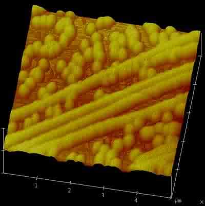
Formation of MoO3 semiconductor nanowires
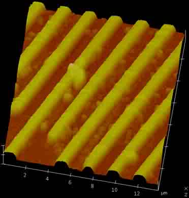
Deposition of Cu and Ni nanowires

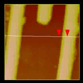
Schematic of monatomic Ni contact formation