 THE DEPARTMENT OF AT STATE
UNIVERSITY OF NEW YORK, POTSDAM N.Y.
THE DEPARTMENT OF AT STATE
UNIVERSITY OF NEW YORK, POTSDAM N.Y.CHEMISTRY
Research with
Students
Students List
Learning through research
Raman Imaging and Spectroscopy Lab
Chemical and Biological Applications of Raman Spectroscopy (pdf, 7 MB)
Quartz Crystal Nanobalance Lab
Studies

Electrochemical Quartz Crystal Nanobalance (EQCN) technique utilizes quartz vibrations and piezoelectric effect to measure mass changes as small as a fraction of a monolayer of atoms
Back to
Professor Maria Hepel
hepelmr@potsdam.edu
Nanotechnology
State University of New York at Potsdam
Stowell Hall
44 Pierrepont Ave.
Potsdam , NY 13676, U.S.A.
Tel.: +1.315.267.2267
Fax: +1.315.267.3170
Chemistry Department of SUNY Potsdam participates actively in this world endeavor by contributing significant research efforts in the following areas:
-
Studies of titanium dioxide nanotubes and mesoporous semiconductive materials for electrochromic devices, solar energy conversion, and for bimetallic catalysts supports in direct methanol fuel cells.
-
Quantum conductance with primary focus on novel phenomena of nanowires and monatomic metal nanobridges.
-
Nanotechnology of single molecule electronic devices
-
Conformational transitions of proteins
-
Nanosensors and ultra-sensitive immunosensors for pesticides and herbicides
-
Environmental studies of photoelectrocatalytic degradation of pollutants
Nanotechnology/Nanoscience Projects
Published Results of Past and Present Projects
The following Nanotechnology/Nanoscience topics have been studied:
1. Controlled interparticle interaction-driven assembly of gold nanoparticles.
|
M. Stobiecka, K. Coopersmith, M. Hepel, "Resonance Elastic Light Scattering (RELS) Spectroscopy of Fast Non-Langmuirian Ligand-Exchange in Glutathione-Induced Gold Nanoparticle Assembly", J. Colloid Interface Science 350 (2010) 168-177. |
||
|
M. Stobiecka, M. Hepel, "Rapid Functionalization of Metal Nanoparticles by moderator-tunable ligand-exchange process for biosensor designs", Sensors Actuators B 149 (2010) 373-380. |
||
|
M. Stobiecka, M. Hepel, "Multimodal Coupling of Optical Transitions and Plasmonic Oscillations in Rhodamine B Modified Gold Nanoparticles", Physical Chemistry Chemical Physics 13 (2011) 1131-1139. |
||
|
M. Stobiecka, M. Hepel, "Ligand Exchange Effects in Gold Nanoparticle Assembly Induced by Oxidative Stress Biomarkers: Homocysteine and Cysteine", Biophysical Chemistry 146 (2010) 98-107. |
2. Study of DNA interactions with drugs and toxicants using DNA microsensors.
|
M. Stobiecka, M. Hepel, "Novel DNA-Hybridization Biosensors for Studies of Atrazine Interactions with DNA", Advances in Environmental Research 6 (2011) 253-298. |
3. Quantum conductance monatomic metal nanobridges.
|
M. Hepel, "Quantum Conductance of Monatomic Ni Nanobridges", Electrochim. Acta 51 (2006) 5811-5824. |
||
|
M. Hepel, "Electrochemical Formation of Quantum Conductance Copper Nanobridges", Elektrokhimiya 44 (2008) 716-729. |
4. Electrochromic display materials.
|
M. Hepel, H. Redmond, I. Dela, "Electrochromic WO3-x Films with Reduced Lattice Deformation Stress and Fast Response Time" Electrochim. Acta 52 (2007) 3541-3549. |
||
| I. Shiyanovskaya, M. Hepel, E. Tewksbury, J. New Mater. Electrochem. Systems, 3 (2000) 241. |
5. Synthesis and characterization of titanium dioxide nanotubes and mesoporous materials for electrocatalysis of methanol in fuel cells and for solar energy conversion devices
|
M. Hepel, I. Kumarihamy, J. Luo, C.J. Zhong, "Novel dynamic efects in methanol oxidation catalysis on nanoporous TiO2-Supported Bimetallic Catalysts for Methanol Oxidation" Electrochimica Acta 52 (2007) 5529-5547. |
||
|
M. Hepel, I. Kumarihamy, C.J. Zhong, "Nanoporous TiO2-Supported Bimetallic Catalysts for Methanol Oxidation in Acidic Media" Electrochem. Commun. 8/9 (2006) 1439-1444. |
||
|
M. Hepel, I. Kumarihamy, "Nanocrystalline Structure and Nanopore Formation in Modified Thermal TiO2 Films" International Journal of Hydrogen Energy 32 (2007) 2693-2702. |
6. Conformational transitions of albumin and interactions of proteins with submonolayer metal films
|
M. Hepel and M. Stobiecka, "Interactions of Addsorbed Albumin with Underpotentially Deposited Copper on Gold Piezoelectrodes" Bioelectrochem. 70 (2007) 155-164. |
||
|
M. Stobiecka, M. Hepel, J. Radecki, "Transient Conformation Changes of Albumin Adsorbed on Gold Piezoelectrodes" Electrochim. Acta 50 (2005) 4873-4887. |
||
|
M. Hepel, "Effect of Albumin on Underpotential Lead Deposition and Stripping on Ag-RDE" Electroanalysis 17 No.15-16 (2005) 1401-1412. |
7. Decomposition of pollutants by photoelectrocatalytic process on nanostructured semiconductor electrodes
|
M. Hepel and S. Hazelton, "Photoelectrochemical Degradation of Diazo Dyes on Nanostructured Electrodes" Electrochim. Acta 50 (2005) 5278-5291. |
8. In-situ Polymerized Conductive Polymers for Nanocomposite Electrocatalysts with Embedded Pt Nanoparticles for Methanol Fuel Cells.
| M. Hepel, J. Electrochem. Soc. , 145 (1998) 124. |
9. Nanotemplating of metal deposition in ion-gate nanochannels.
M. Hepel, E. Tewksbury, Electrochim. Acta, 49 (2004) 3827;
M. Hepel, E. Tewksbury, J. Electroanal. Chem., 552 (2003) 291;
M. Hepel, J. Electroanal. Chem, 509 (2001) 90.
10. Electrocatalytic properties of gold nanoparticles with 2-5 nm size.
J. Luo, M. Maye, Y. Lou, L. Han, M. Hepel, C. Zhong, Catalysis Today, 77 (2002) 127.
11. Controlled drug release from conductive polymer matrix.
M. Hepel, F. Mahdavi, Microchem. Journal, 56 (1997) 54.
12. Development of piezoelectric immunosensors based on molecular surface structure design.
J. Pribyl, M. Hepel, J. Halamek, P. Skladal, Sensors and Actuators, B91 (2003) 333.
13. Deposition of metal films with silicon carbide nanoparticles for increased hardness and corrosion resistance.
M. Hepel and Christine Mahoney, Electrochem. Glass and Ceramics, Ceramics Trans., 92 (1999) 303.
14. Semiconductor nanowires of WO3 and MoO3.
Published Abstract at the Electrochemical Soc. Meeting, Quebec City, Canada, May 2005.
Examples of Nanoscience / Nanotechnology topics
included in undergraduate teaching science courses
during last two years (2003-2005)
1. Demonstration of atomic forces between molecules including friction imaging.
2. Imaging of bacteria upon chemical treatment using Atomic Force Microscopy, in collaboration with Biology Department.
3. Imaging of collagen fibers using Atomic force Microscopy, in collaboration with Biology Department.
4. Deposition of nanowires on atomic steps on a highly oriented pyrolytic graphite surface (HOPG).
5. Piezosensors for detection of heavy metals and pesticides.
6. Imaging of surface of monolayer films using Atomic Force Microscopy and Scanning Tunneling Microscopy
7. Imaging of interdigitated nanosensor structure by tapping-mode
Atomic Force Microscopy.
8. Effect of corrosion inhibitors on micro- and nano-corrosion of
metals.
Research and Teaching Projects in Nanoscience / Nanotechnology
(Current and Planned Projects)
-
Synthesis of gold and silver nanoparticles (5 - 40 nm dia.) and nonorods with aspect ratio 2:1 and 4:1 and the analysis of surface plasmon spectral absorbance shift dependent on particle size and shape.
-
Monitoring gold nanoparticle assembly using resonance elastic light scattering (RELS) spectroscopy.
-
Preparation and testing of metal and semiconductor nanowires and nanobridges for electronic applications.
-
Templated metal deposition, e.g. copper, nickel, cadmium
-
Preparation and testing of composite TiO2 nanostructured materials for solar-hydrogen cells.
-
Use of modified gold nanoparticles as nanosensors for biomolecules detection.
-
Preparation and testing of semiconductor nanostructured WO3, MoO3 materials for degradation of pollutants and electrochromic applications.
-
Use of modified gold nanoparticles as nanosenors for biomolecules detection.
-
Development of nanosensor arrays for heavy metals detection.
-
Defective genes detection and DNA hybridization using DNA microsensors.
-
Nanosensors for detecting drugs, lipids, and cations binding to proteins and DNA binding to proteins.
Available equipment to be used in these projects is:
-
Atomic Force Microscope (AFM) / Scanning Tunneling Microscope (STM)
-
Dispersive Raman Spectrometer and Raman Microscope
-
Electrochemical Quartz Crystal Nanonalance (EQCN)
-
High Frequency Immittance Spectroscopy Analyzer (QCI).
-
Fluorescence Spectrophotometer.
-
UV-vis and FTIR Spectrophotometers.

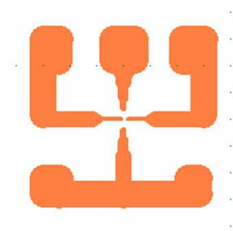
Electrochemistry on a microchip
Microprinted circuits for studies of nanowires and molecular electronic devices use sub-microliter solution volume
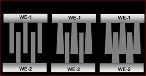
Quantum Conductance Monatomic Nanobridge Devices
studied using conductanc spectroscopy and AFM/STM

Nanowires of a semiconductor MoO3
obtained by eletrochemical deposition from peroxo-complexes of Mo(VI)
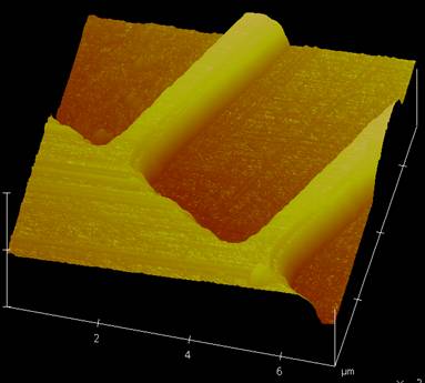
Microelectrode circuit
AFM image of microelectrode circuit used in quantum conductance studies of Ni monatomic nanobridges
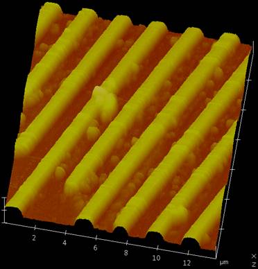
Interdigitated electrodes
AFM image of an interdigitated electrode pattern for capacitive nanosensors